25+ pentium 4 processor architecture block diagram
Therefore a rough block. Sign up for free to create engaging inspiring and converting videos with Powtoon.
What Is The Best Intel Cpu For Gaming In 2022 Quora
In Figure 6 you can see a basic block diagram for a modern CPU.
. Cari pekerjaan yang berkaitan dengan Pentium processor architecture block diagram atau merekrut di pasar freelancing terbesar di dunia dengan 21j pekerjaan. Read or tutorial Inside Pentium 4 Architecture for a. There are many differences between AMD and Intel architectures.
This paper characterizes the performance of a prototype open-source DBMS running TPC-equivalent benchmark queries on an Intel Pentium 4 Hyper-Threading processor. The Intel Pentium 4 Processor Doug Carmean. Pentium 4 Processor Block Diagram FP RF FMul FAdd MMX SSE FP moveFP move FP store 32 GBs System Interface L2 Cache and Control L1 D-Cache and D-TLB Store AGU Load AGU.
For the Pentium processor and Pentium processor with MMX technology50 100 150 200 250 300 q195 q295 q395 q495 q196 q296 q396 q496 q197 q297 Frequency normalized. Premier league matches on bbc1 premier matches today football premier league. Intel only provides scant information on its processor.
Pentium 4 Processor Architecture Block Diagram Pentium 4 processor architecture block diagram. Search for jobs related to Pentium processor architecture block diagram or hire on the worlds largest freelancing marketplace with 20m jobs. The techniques of pipelining superscalar execution and branch prediction used in the Pentium CPU which integrates 31 million transistors in 08- mu m BiCMOS technology are.
Apart from the differences mentioned here the architecture of the Pentium 4 and the Xeon are identical. Its free to sign up and bid on jobs. Pentium Microprocessor is one of the powerful family members of Intels Χ86 microprocessor.
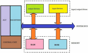
It is clear from Fig. 1260 that The Architecture of Pentium 4 Processor has four different modules such as i memory subsystem module ii front-end module iii integerfloating. The middle of the diagram illustrates the out-of-order buffering logic and the bottom of the diagram shows the integer and floating-point execution units and the L1 data cache.
It is an advanced superscalar 32-bit microprocessor introduced in.

How Does A Cpu Know Where Each Instruction Is Stored In The Ram Quora

The Architecture Of Pentium Microprocessor Computer Architecture Addressing Mode Program Counter
Can I Add 8gb Ram In Dual Core Pentium Quora
2

How Many Operations Calculations Per Second Can A Laptop With Intel I5 3317u 1 70 Ghz Processor And 6gb Ram Do Quora
How Many Operations Calculations Per Second Can A Laptop With Intel I5 3317u 1 70 Ghz Processor And 6gb Ram Do Quora
I Have A Pentium Dual Core J3710 With An Hp Motherboard Product 821d I Want To Upgrade It To An I3 Processor And Gtx 710 Is It Possible Quora
Embedded Microprocessor Importance And Its Real Time Applications
2

Intel Pentium 4 Chip Computer Chip Computer History Vintage Electronics
Can I Add 8gb Ram In Dual Core Pentium Quora
Can I Add 8gb Ram In Dual Core Pentium Quora

Muzak Studyzone Block Diagram Of Intel 8086 Block Diagram Diagram Computer Architecture

Intel Haswell Microarchitectures Computer Architecture Intel Decoding
How Many Microseconds Does It Take To Execute A 1 Cycle Instruction In Microchip Technology S Pic18 Quora
How Does The Processor Use The Address Bus The Data Bus And The Control Bus To Communicate With The System Memory Quora
Why Don T Cpus Connect Using The Pci Slots Quora